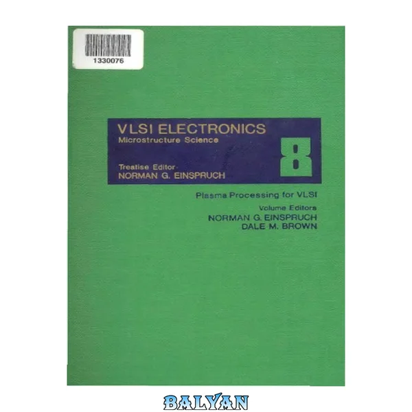
Beam Processing Technologies is a collection of papers that deals with the miniaturization of devices that will be faster, consume less power, and cost less per operation or fabrication. One paper discusses metal oxide semiconductor (MOS) integrated circuit technology including the operation of devices whose lateral and vertical dimensions are scaled down. If the devices'silicon doping profiles are increased by the same scale factor, they can operate on lower voltages and currents, with the same performance. Another paper describes laser beam processing and wafer-scale integration as techniques to increase the number of devices on a silicon chip. Electron beam technologies can be used in many fabrication processes such as in microlithography, selective oxidation, doping, metrology. Ion beam applications depend on the presence of the ion introduced into the device (e.g. implantation doping), on pseudoelastic collisions (e.g. physical sputtering or crystal damage), and on inelastic scattering (e.g. polymer resist exposure). Silicon molecular beam epitaxy (SiMBE) can also grow high-quality layers at low temperature, particularly concerning germanium, especially as reagrds the growth system design and utilization of n- and p-type doping. Chemical beam epitaxy (CBE) is another epitaxial growth technique that can surpass MBE and metal organic chemical vapor deposition (MO-CVD). The collection is suitable chemical engineers, industrial physicists, and researchers whose work involve micro-fabrication and development of integrated circuits. V. 1-5. [without Special Title] -- V. 6. Materials And Process Characterization -- V. 7. [without Special Title] -- V. 8. Plasma Processing For Vlsi -- V. 9. [without Special Title] -- V. 10. Surface And Interface Effects In Vlsi -- V. 11. Gaas Microelectronics -- V. 12. Silicon Materials -- V. 13. Metal-semiconductor Contacts And Devices -- V. 14. Vlsi Design -- V. 15. Vlsi Metallization -- V. 16. Lithography For Vlsi -- V. 17. Vlsi In Medicine -- V. 18. Advanced Mos Device Physics -- V. 19. Advanced Cmos Process Technology -- 20. Vlsi And Computer Architecture -- V. 21. Beam Processing Technologies -- V. 22. Vlsi Reliability -- V. 23. Application Specific Integrated Circuit (asic) Technology -- V. 24. Heterostructures And Quantum Devices. Edited By Norman G. Einspruch. Includes Bibliographical References And Index. v. 1-5. [without special titles] v. 6. Materials and process characterization v. 7. [without special title] v. 8. Plasma processing for VLSI v. 9. [without special title] v. 10. Surface and interface effects in VLSI v. 11. GaAs microelectronics v. 12. Silicon materials v. 13. Metal-semiconductor contacts and devices v. 14. VLSI design v. 15. VLSI metallization v. 16. Lithography for VLSI v. 17. VLSI in medicine v.18. Advanced MOS device physics 19. Advanced CMOS process technology v. 21. Beam processing technologies v. 22. VLSI reliability v. 23. Application specific integrated circuit (ASIC) technology v. 24. Heterostructures and quantum devices. Presents a survey of current developments in ASIC technology, addressed from the viewpoints of both ASIC vendor and user. Topics covered include ASIC business, marketing, design, CAD, manufacturing, and application and selection of ASICs.